LTC6951IUHF#PBF, Clock Synthesizer / Jitter Cleaner Ultralow Jitter Multi-Out Clock Synthesi
Изображения служат только для ознакомления,
см. техническую документацию
см. техническую документацию

25 300 ֏
от 10 шт. —
20 800 ֏
от 25 шт. —
19 900 ֏
от 104 шт. —
16 500 ֏
Добавить в корзину 1 шт.
на сумму 25 300 ֏

Описание
Semiconductors\Clock & Timer ICs\Clock Synthesizer / Jitter Cleaner
LTC695x Ultra-low Jitter Clock SynthesizersAnalog Devices Inc. LTC695x Ultra-low Jitter Clock Synthesizers offer designers clocking solutions that help maximize the data converter signal-to-noise ratio (SNR). The LTC695x Ultra-low Jitter Clock Synthesizers are easily synchronized using the Analog Devices synchronization programs. The EZSync™ multi-chip synchronization ensures consistent edge alignment across all outputs. ParallelSync™ multi-chip parallel synchronization allows designers to re-time the outputs of multiple ICs to the common reference clock. This process enables reference-aligned synchronization in the reference clock domain with an easy-to-meet nanosecond range setup and holds time requirements.
Технические параметры
| Brand: | Analog Devices |
| Factory Pack Quantity: Factory Pack Quantity: | 52 |
| Manufacturer: | Analog Devices Inc. |
| Max Output Freq: | 2.5 GHz |
| Maximum Input Frequency: | 425 MHz |
| Maximum Operating Temperature: | +105 C |
| Minimum Operating Temperature: | -40 C |
| Mounting Style: | SMD/SMT |
| Number of Outputs: | 5 Output |
| Operating Supply Current: | 210 mA |
| Output Level: | CML, LVDS |
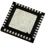
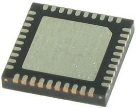
| Package / Case: | QFN-40 |
| Packaging: | Tube |
| Product Category: | Clock Synthesizer/Jitter Cleaner |
| Product Type: | Clock Synthesizers/Jitter Cleaners |
| Product: | Clock Synthesizers |
| Series: | LTC6951 |
| Subcategory: | Clock & Timer ICs |
| Supply Voltage - Max: | 5.25 V |
| Supply Voltage - Min: | 3.15 V |
| Type: | Low Jitter |
| Automotive | No |
| Clock Input Frequency (MHz) | 2 to 425 |
| ECCN (US) | EAR99 |
| EU RoHS | Compliant |
| Input Logic Level | CML|CMOS|LVDS|LVPECL |
| Lead Shape | No Lead |
| Maximum Operating Supply Voltage (V) | 3.45 |
| Maximum Operating Temperature (°C) | 105 |
| Maximum Output Frequency (MHz) | 2500 |
| Maximum Supply Current (mA) | 130 |
| Minimum Operating Supply Voltage (V) | 3.15 |
| Minimum Operating Temperature (°C) | -40 |
| Mounting | Surface Mount |
| Number of Outputs per Chip | 5 |
| Output Logic Level | CML|LVDS |
| Packaging | Tube |
| Part Status | Active |
| PCB changed | 40 |
| Pin Count | 40 |
| PPAP | No |
| Standard Package Name | QFN |
| Supplier Package | QFN EP |
| Typical Duty Cycle (%) | 50 |
| Differential - Input | Output |
| Divider/Multiplier | Yes/No |
| Frequency - Max | 2.5GHz |
| Input | Clock |
| Manufacturer | Linear Technology |
| Mounting Type | Surface Mount |
| Number of Circuits | 1 |
| Operating Temperature | -40В°C ~ 105В°C |
| Output | CML, LVDS |
| Package / Case | 40-WFQFN Exposed Pad |
| PLL | Yes |
| Ratio - Input | Output |
| Series | - |
| Standard Package | 52 |
| Supplier Device Package | 40-QFN(7x5) |
| Voltage - Supply | 3.15 V ~ 3.45 V |
| Вес, г | 0.1 |
Техническая документация
Похожие товары
![M48T08-150PC1, Часы реального времени TIMEKEEPER, SRAM 64Кбит (8Кбx8), 5В, [PCDIP-28]](https://static.chipdip.ru/lib/006/DOC001006527.jpg)
![DS1248Y-70, Микросхема, 1024K NV SRAM with Phantom Clock [DIP-32]](https://static.chipdip.ru/lib/141/DOC001141484.jpg)