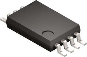
CDCLVC1102PW, CDCLVC1102PW PLL Clock Buffer 8-Pin TSSOP

Изображения служат только для ознакомления,
см. техническую документацию
см. техническую документацию


2 270 ֏
Кратность заказа 150 шт.
Добавить в корзину 150 шт.
на сумму 340 500 ֏
Описание
Semiconductors\Clock, Timing & Frequency ICs\Clock Buffers
Clock Buffers from Texas Instruments combine low additive jitter and skew with highly flexible input/output formats which make it easy to distribute clock signals.
Технические параметры
| Maximum Input Frequency | 180 MHz, 250 MHz |
| Maximum Operating Supply Voltage | 2.7 V, 3.6 V |
| Maximum Operating Temperature | +85 °C |
| Maximum Output Frequency | 180 MHz, 250 MHz |
| Maximum Supply Current | 10 mA |
| Minimum Operating Supply Voltage | 2.3 V, 3 V |
| Minimum Operating Temperature | -40 °C |
| Mounting Type | Surface Mount |
| Number of Elements per Chip | 6 |
| Package Type | TSSOP |
| Pin Count | 8 |
| Width | 3.1mm |
| Brand | Texas Instruments |
| Factory Pack Quantity | 150 |
| Input Type | LVCMOS |
| Manufacturer | Texas Instruments |
| Max Output Freq | 250 MHz |
| Mounting Style | SMD/SMT |
| Number of Outputs | 2 Output |
| Operating Supply Current | 6 mA |
| Output Type | LVCMOS |
| Package / Case | TSSOP-8 |
| Packaging | Tube |
| Product Category | Clock Buffer |
| Propagation Delay - Max | 2.6 ns |
| RoHS | Details |
| Series | CDCLVC1102 |
| Supply Voltage - Max | 2.7 V, 3.6 V |
| Supply Voltage - Min | 2.3 V, 3 V |
| Unit Weight | 0.005573 oz |
| Brand: | Texas Instruments |
| Factory Pack Quantity: Factory Pack Quantity: | 150 |
| Input Type: | LVCMOS |
| Manufacturer: | Texas Instruments |
| Max Output Freq: | 250 MHz |
| Maximum Input Frequency: | 250 MHz |
| Maximum Operating Temperature: | +85 C |
| Minimum Operating Temperature: | -40 C |
| Mounting Style: | SMD/SMT |
| Number of Outputs: | 2 Output |
| Operating Supply Current: | 6 mA |
| Output Type: | LVCMOS |
| Package / Case: | TSSOP-8 |
| Packaging: | Tube |
| Product Category: | Clock Buffer |
| Product Type: | Clock Buffers |
| Product: | Clock Buffers |
| Propagation Delay - Max: | 2 ns |
| Series: | CDCLVC1102 |
| Subcategory: | Clock & Timer ICs |
| Supply Voltage - Max: | 3.6 V |
| Supply Voltage - Min: | 2.3 V |
| Absolute Propagation Delay Time (ns) | 10 |
| Automotive | No |
| ECCN (US) | EAR99 |
| EU RoHS | Compliant |
| Fanout | 1:2 |
| Input Logic Level | LVCMOS |
| Lead Shape | Gull-wing |
| Maximum Operating Supply Voltage (V) | 3.6 |
| Maximum Operating Temperature (°C) | 85 |
| Maximum Propagation Delay Time @ Maximum CL (ns) | 2.6@2.5V|2@3.3V |
| Minimum Operating Supply Voltage (V) | 2.3 |
| Minimum Operating Temperature (°C) | -40 |
| Mounting | Surface Mount |
| Number of Outputs per Chip | 2 |
| Output Logic Level | LVCMOS |
| Part Status | Active |
| PCB changed | 8 |
| PPAP | No |
| Standard Package Name | SOP |
| Supplier Package | TSSOP |
| Type | Fanout Buffer |
| Typical Operating Supply Voltage (V) | 2.5|3.3 |


